
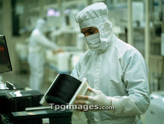
Semiconductor manufacture. Technician in a clean room facility inspecting silicon wafers for use in semiconductor devices in the electronics industry. The wafers must be made from high-quality crystals of precisely controlled orientation and electrical properties. Photographed in Germany.
| px | px | dpi | = | cm | x | cm | = | MB |
Details
Creative#:
TOP03226823
Source:
達志影像
Authorization Type:
RM
Release Information:
須由TPG 完整授權
Model Release:
N/A
Property Release:
N/A
Right to Privacy:
No
Same folder images:
 Loading